Bump on Pad, Wafer Process Technology
$ 17.99 · 4.8 (533) · In stock
Bump on Pad Key features include: Wafer process and bumping in consolidated assembly. Technology supporting wide range of products from mobile devices to
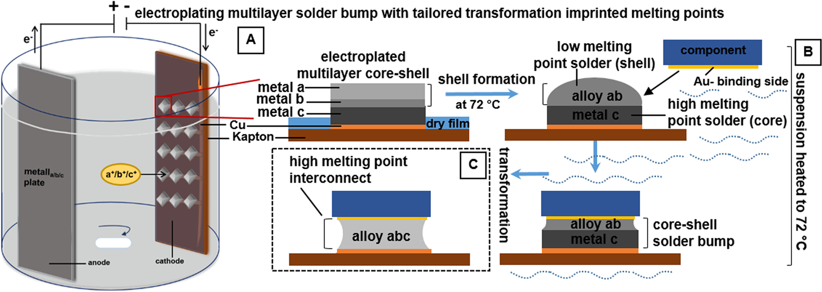
Fluidic Self-Assembly on Electroplated Multilayer Solder Bumps with Tailored Transformation Imprinted Melting Points
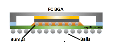
Understanding Wafer Bumping Packaging Technology - AnySilicon
Prestige Popular Stainless Steel Pressure Cooker, Litres
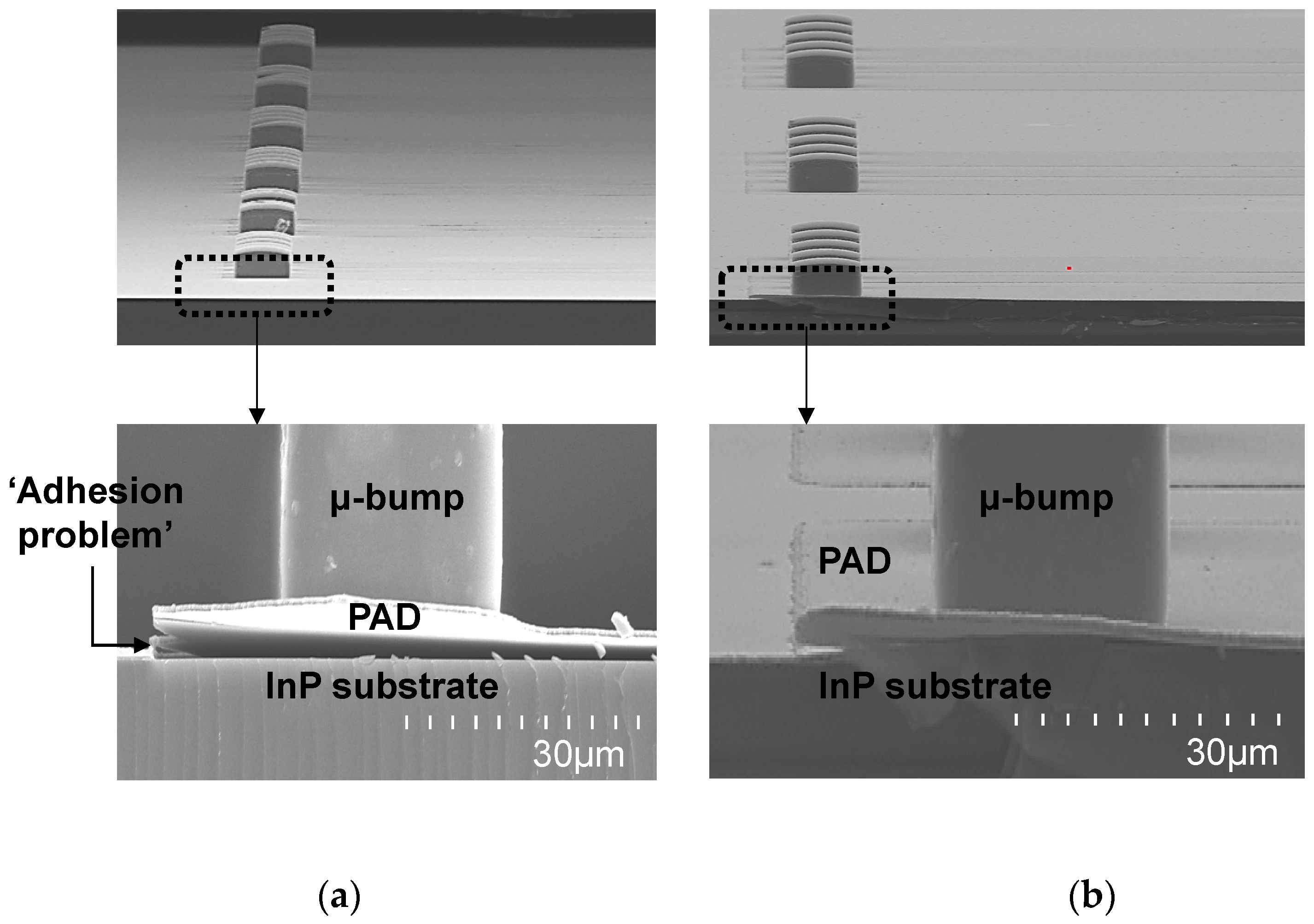
Micromachines, Free Full-Text

Process and Key Technology of Typical Advanced Packaging
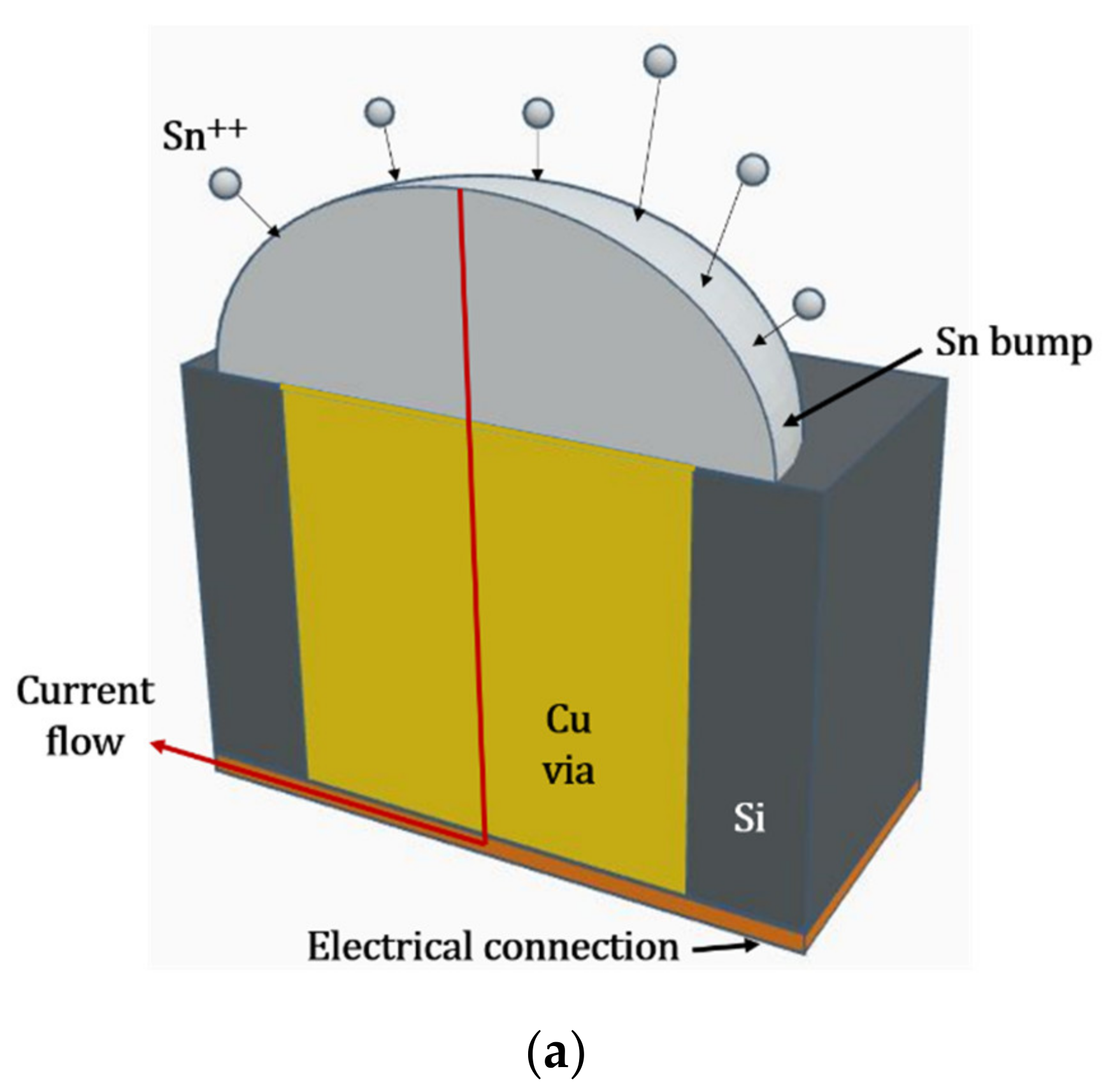
Metals, Free Full-Text
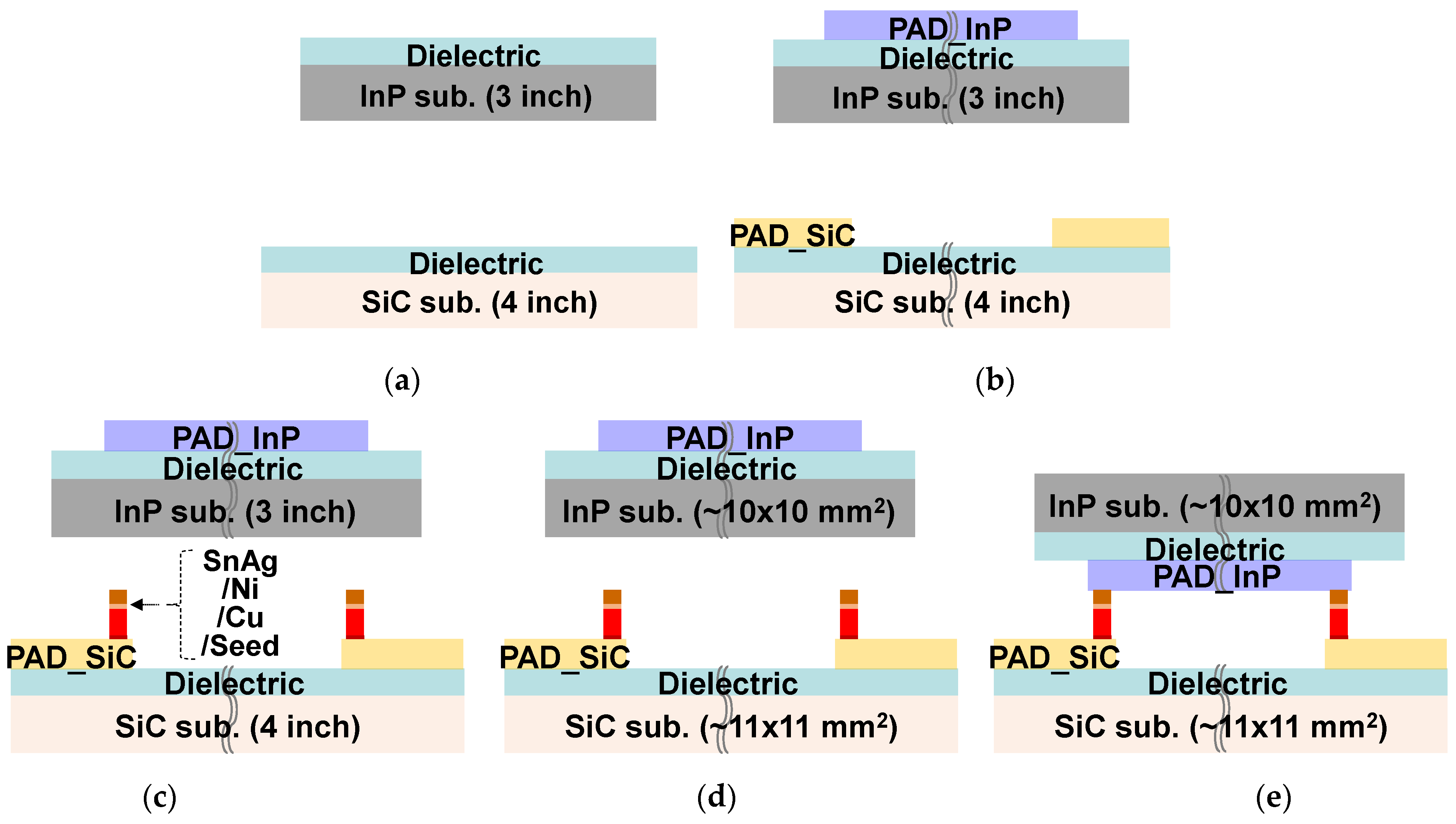
Micromachines, Free Full-Text

Semiconductor Back-end Process 3: Packages

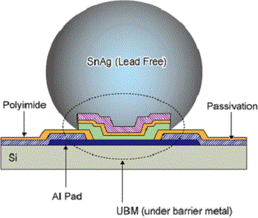
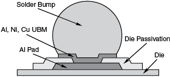
The bond pad redistribution layer (polyimide 1) and the under bump
Tech Brief: Primer on Packaging
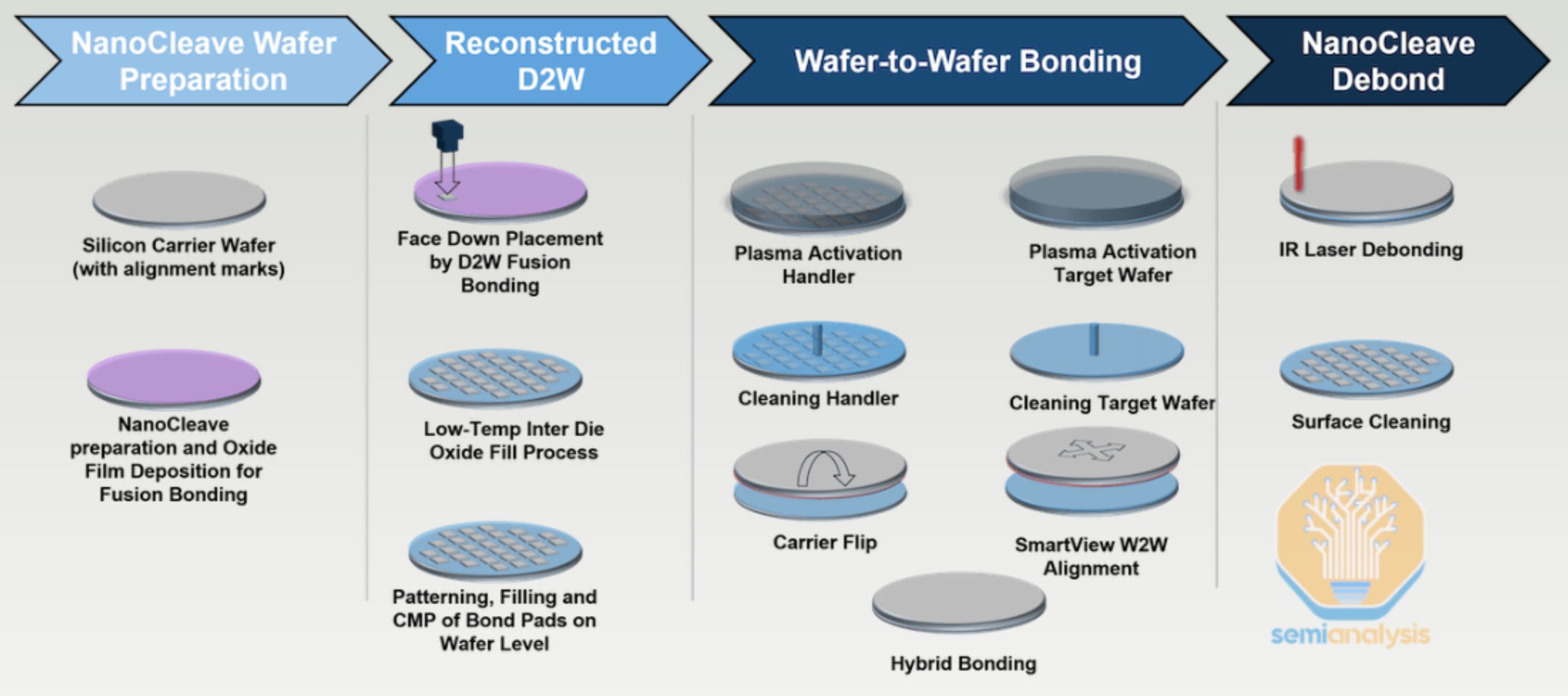
Hybrid Bonding Process Flow - Advanced Packaging Part 5
Flip Chips-Pac Tech Dummy Components

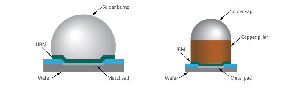
Evaporation UBM and solder bumping process. of tin deposited separately