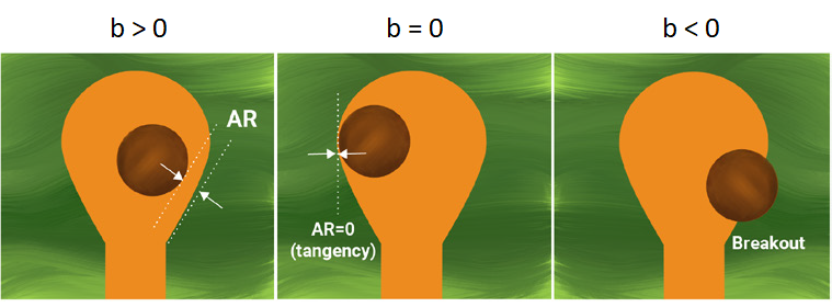
PCB Via Size and Pad Size Guidelines, Zach Peterson
$ 6.00 · 4.8 (546) · In stock
Do you know what PCB via size you should use in your PCB layout? We’ll look at a few simple ways to answer this question.
PCB Via Size and Pad Size Guidelines, Zach Peterson, Blog
ESR_Calculators__th.jpg

3210 PDFs Review articles in PCB DESIGN

US9465412B2 - Input device layers and nesting - Google Patents

PCB GraphTech Pte Ltd

US9465412B2 - Input device layers and nesting - Google Patents
Why Most Via Impedance Calculators Are Inaccurate, Zach Peterson
PCB Via Size and Pad Size Guidelines, Zach Peterson, Blog

PCB GraphTech Pte Ltd

Design007 Magazine :: I-Connect007

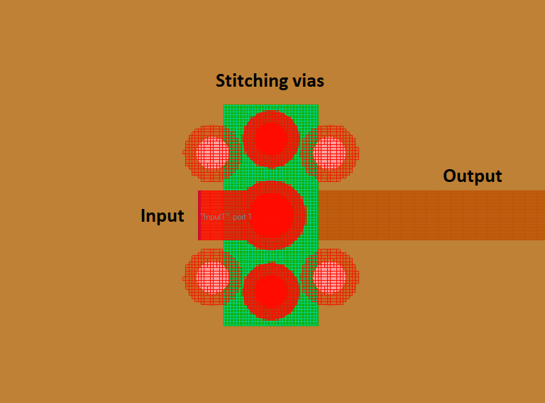
Routing with Vias PCB Routing