a) Under-bump metallization and micro-bumps fabricated on the VLSI
$ 12.50 · 4.6 (354) · In stock


Impact of TSV bump and redistribution layer on crosstalk delay and

Stevan DJORDJEVIC, Principal Silicon Photonic Engineer

Mehdi ASGHARI KHIAVI, University of Toronto, Toronto

Experimental investigation of electromigration failure in Cu–Sn–Cu

PDF) Microring-based multi-chip WDM photonic module

Materials, Free Full-Text

US20120091576A1 - Under-bump metallization (ubm) structure and

a) Under-bump metallization and micro-bumps fabricated on the VLSI

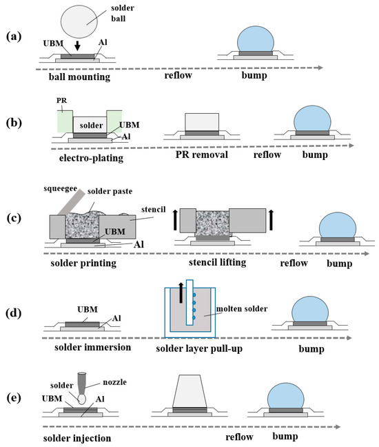
Eng Sub] Wafer Bumping Process: Solder bump, Cu pillar bump, UBM
Roshanak SHAFIIHA, Staff Engineer, PhD, R&D
All about Fan-In & Fan-Out Wafer-Level Package (WLP)
Materials, Free Full-Text
Shear test evaluation of the mechanical reliability of micro bumps
Xuezhe ZHENG, Managing Director, Ph.D

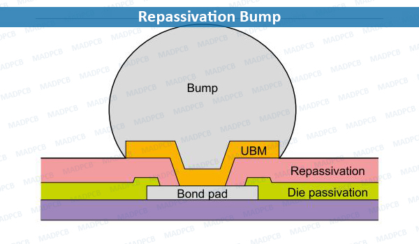
UBM (under bump metallurgy) structure